| CPC H01L 25/18 (2013.01) [H01L 24/05 (2013.01); H01L 24/08 (2013.01); H01L 24/32 (2013.01); H01L 24/83 (2013.01); H01L 24/94 (2013.01); H01L 25/50 (2013.01); H01L 2224/05647 (2013.01); H01L 2224/08145 (2013.01); H01L 2224/32054 (2013.01); H01L 2224/32059 (2013.01); H01L 2224/32145 (2013.01); H01L 2224/80203 (2013.01); H01L 2224/83139 (2013.01); H01L 2224/83203 (2013.01)] | 20 Claims |

|
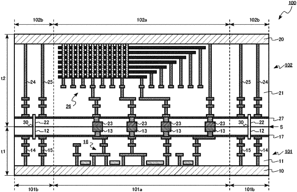
1. A manufacturing method of a semiconductor device, comprising:
attaching a first substrate to a second substrate, wherein
the first substrate includes:
a first element region,
a first peripheral region that surrounds the first element region,
a first insulator in the first element region and the first peripheral region and having a first recess portion in the first peripheral region,
a first metal layer in the first element region and exposed at an uppermost surface of the first substrate,
a first conductor in the first peripheral region in the first insulator below the uppermost surface of the first substrate, the first conductor surrounding the first element region, and
a first insulating layer between the first conductor and the interface between the first substrate and the second substrate, the first insulating layer comprising silicon and nitrogen;
the second substrate includes:
a second element region,
a second peripheral region that surrounds the second element region,
a second insulator in the second element region and the second peripheral region, the second insulator having a second recess portion in the second peripheral region,
a second metal layer in the second element region and exposed at an uppermost surface of the second substrate,
a second conductor in the second peripheral region in the second insulator below the uppermost surface of the second substrate, the second conductor surrounding the second element region, and
a second insulating layer between the second conductor and the interface between the first substrate and the second substrate, the second insulating layer comprising silicon and nitrogen; and
after the first substrate and the second substrate are attached, the first metal layer and the second metal layer directly contact one another, and the first recess portion and the second recess portion are connected to one another.
|