| CPC H01L 25/18 (2013.01) [G11C 14/0018 (2013.01); G11C 16/04 (2013.01); H01L 23/481 (2013.01); H01L 23/5226 (2013.01); H01L 25/50 (2013.01); H10B 41/27 (2023.02); H10B 43/27 (2023.02); G11C 13/0004 (2013.01); H10B 41/41 (2023.02)] | 20 Claims |

|
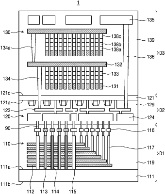
1. A method of fabricating a fusion memory device, the method comprising:
forming a first memory cell circuit including a plurality of first memory cells on an active surface of a first substrate;
forming a non-memory circuit including a plurality of conductive lines on an active surface of a second substrate;
combining the first memory cell circuit with the non-memory circuit; and
forming a second memory cell circuit including a plurality of second memory cells on an inactive surface of the second substrate,
wherein forming the first memory cell circuit and forming the non-memory circuit are performed independently of each other, and
wherein forming the first memory cell circuit is performed at a first temperature higher than a second temperature of forming the second memory cell circuit, and
wherein forming the second memory cell circuit does not include a diffusion process.
|