| CPC H01L 25/0657 (2013.01) [H01L 21/565 (2013.01); H01L 21/76898 (2013.01); H01L 21/78 (2013.01); H01L 22/12 (2013.01); H01L 22/32 (2013.01); H01L 23/481 (2013.01); H01L 24/14 (2013.01); H01L 25/18 (2013.01); H01L 25/50 (2013.01); H01L 2224/14517 (2013.01); H01L 2225/06513 (2013.01); H01L 2225/06541 (2013.01); H01L 2225/06586 (2013.01); H01L 2225/06596 (2013.01)] | 20 Claims |
|
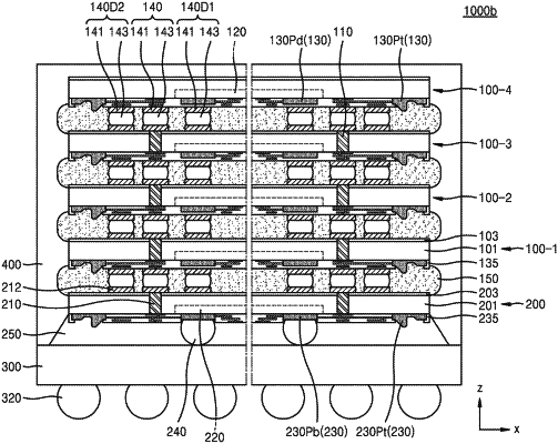
1. A semiconductor package comprising:
an interface chip comprising a first pad provided in an outer portion of the interface chip, a second pad provided inside the first pad, and a first through silicon via (TSV) provided between the first pad and the second pad;
at least one memory chip stacked on the interface chip, wherein the at least one memory chip comprises a third pad provided in an outer portion of the at least one memory chip, a fourth pad provided inside the third pad, and a second TSV provided between the third pad and the fourth pad; and
an adhesive layer provided between the interface chip and the at least one memory chip,
wherein a first bump is provided on the second pad on a bottom surface of the interface chip,
a second bump is provided on the second TSV on a bottom surface of the at least one memory chip,
a dummy bump is provided on the bottom surface of the at least one memory chip to be adjacent to the second bump, and
each of the first pad and the third pad comprises a groove.
|