| CPC H01L 24/81 (2013.01) [H01L 24/13 (2013.01); H01L 24/16 (2013.01); H01L 25/0657 (2013.01); H01L 2224/13082 (2013.01); H01L 2224/13111 (2013.01); H01L 2224/13147 (2013.01); H01L 2224/13155 (2013.01); H01L 2224/16227 (2013.01); H01L 2224/81201 (2013.01); H01L 2224/81815 (2013.01); H01L 2225/06506 (2013.01); H01L 2225/0651 (2013.01); H01L 2225/06517 (2013.01); H01L 2225/06562 (2013.01); H01L 2225/06575 (2013.01); H01L 2225/06582 (2013.01)] | 20 Claims |

|
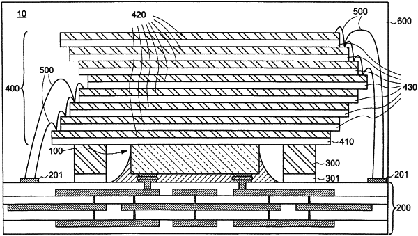
1. A method of manufacturing a semiconductor device, the method comprising:
forming a metal bump on a first surface side of a semiconductor chip;
positioning the semiconductor chip so the metal bump contacts a pad of an interconnection substrate;
applying a first light from a second surface side of the semiconductor chip and melting the metal bump with the first light;
allowing the melted metal bump to resolidify by stopping or reducing the application of the first light;
pressing the semiconductor chip toward the interconnection substrate after the stopping or reducing of the application of the first light;
applying a second light from the second surface side of the semiconductor chip while pressing the semiconductor chip toward the interconnection substrate to melt the metal bump; and
allowing the melted metal bump to resolidify by stopping or reducing the application of the second light, wherein
the application of the second light is started after the pressing of the semiconductor chip toward the interconnection substrate begins, and
the pressing of the semiconductor chip toward the interconnection substrate is stopped after the stopping or reducing of the application of the second light.
|