| CPC H01L 24/05 (2013.01) [H01L 24/03 (2013.01); H01L 2224/039 (2013.01); H01L 2224/05017 (2013.01); H01L 2224/05082 (2013.01); H01L 2224/05083 (2013.01); H01L 2224/05084 (2013.01); H01L 2224/05124 (2013.01); H01L 2224/05155 (2013.01); H01L 2224/0566 (2013.01); H01L 2924/35121 (2013.01)] | 16 Claims |

|
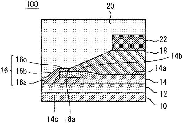
1. A semiconductor device, comprising:
a semiconductor substrate;
a first electrode provided on the semiconductor substrate;
an insulating layer including a first part provided on an upper surface of the first electrode;
a second electrode including a main portion and an eaves portion, the main portion being provided on the upper surface of the first electrode, the eaves portion being connected to the main portion and extending over the first part; and
solder covering and directly contacting an upper surface of the main portion and a part of an uppermost surface of the eaves portion connected with the upper surface of the main portion of the second electrode;
wherein
the insulating layer includes:
a second part covering a part of the uppermost surface of the eaves portion, the part being closer to an end of the eaves portion than the part covered by the solder; and
a third part connecting the first part and the second part and covering the end of the eaves portion, and
a length of the second part from the end of the eaves to an end of the second part is shorter than a length of the first part from the end of the eaves portion to an end of the first part.
|