| CPC H01L 23/5389 (2013.01) [H01L 23/3128 (2013.01); H01L 23/49811 (2013.01); H01L 23/49822 (2013.01); H01L 23/49838 (2013.01); H01L 23/5383 (2013.01); H01L 24/16 (2013.01); H01L 25/105 (2013.01); H01L 2224/16225 (2013.01)] | 20 Claims |

|
1. A method for manufacturing a semiconductor package, comprising:
forming a redistribution substrate; and
placing a semiconductor chip on the redistribution substrate,
wherein the forming a redistribution substrate includes,
forming an under-bump pattern,
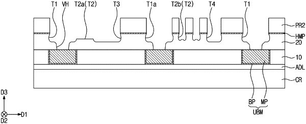
forming a first photo-imageable dielectric layer including a preliminary via hole exposing the under-bump pattern on the under-bump pattern,
forming a first hard mask layer covering the first photo-imageable dielectric layer and the under-bump pattern, wherein the first hard mask partially fills the preliminary via hole,
etching the first hard mask layer and the first photo-imageable dielectric layer sequentially to remove the first hard mask layer in the preliminary via hole and form a via hole from the preliminary via hole and a first hole vertically overlapping and connecting with the via hole,
removing the first hard mask layer,
forming a first seed/barrier layer and a first metal layer sequentially to fill the via hole and the first hole, and
performing a planarization process on the first seed/barrier layer and the first metal layer to form a redistribution pattern.
|