| CPC H01L 23/5386 (2013.01) [H01L 23/3128 (2013.01); H01L 23/49816 (2013.01); H01L 23/49822 (2013.01); H01L 23/49833 (2013.01); H01L 23/49838 (2013.01); H01L 23/5385 (2013.01); H01L 24/08 (2013.01); H01L 24/73 (2013.01); H01L 25/0657 (2013.01); H01L 2224/08235 (2013.01); H01L 2224/73204 (2013.01); H01L 2225/06517 (2013.01); H01L 2225/0652 (2013.01)] | 20 Claims |
|
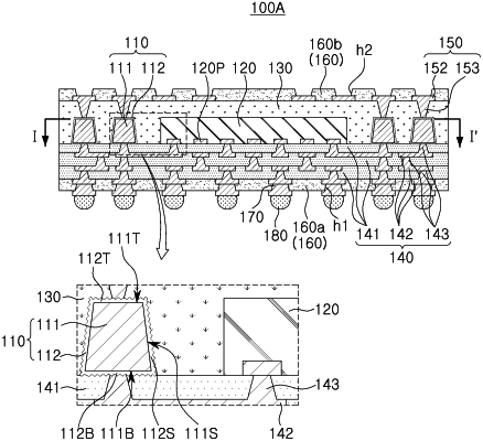
1. A semiconductor package comprising:
a redistribution substrate comprising a first redistribution layer;
a semiconductor chip on the redistribution substrate and electrically connected to the first redistribution layer;
at least one vertical connection structure adjacent the semiconductor chip and having a first surface roughness;
a core structure on the redistribution substrate and having a first through-hole in which the semiconductor chip is disposed, at least one second through-hole in which the at least one vertical connection structure is disposed, and a second surface roughness;
an encapsulant on the redistribution substrate, the semiconductor chip, the core structure, and the at least one vertical connection structure; and
a redistribution structure on the encapsulant and comprising a second redistribution layer,
wherein the at least one vertical connection structure is electrically connected to the first redistribution layer at a bottom surface thereof and the second redistribution layer at a top surface thereof, and
the core structure is electrically insulated to the first redistribution layer and the second redistribution layer.
|