| CPC H01L 23/528 (2013.01) [H01L 21/823475 (2013.01); H01L 25/105 (2013.01); H01L 27/088 (2013.01); H01L 29/401 (2013.01); H01L 29/41725 (2013.01); H03K 17/6871 (2013.01)] | 18 Claims |
|
1. A semiconductor device, comprising:
a primary transistor formed within a semiconductor substrate, the primary transistor having a first current terminal, a second current terminal, and a control terminal;
a reference transistor adjacent to the primary transistor formed within the semiconductor substrate, the reference transistor having a first current terminal, a second current terminal, and a control terminal; and
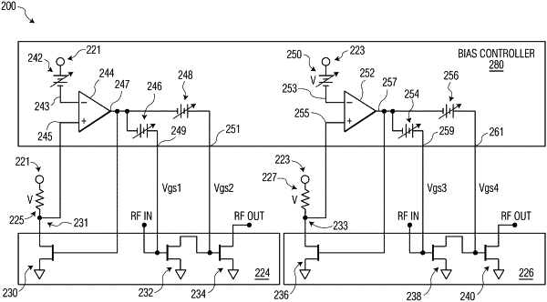
a bias controller configured to operate the primary transistor at a desired operating point by:
applying predetermined bias voltages to the current terminals and the control terminal of the reference transistor;
measuring a reference electrical current level flowing between the first current terminal and the second current terminal of the reference transistor; and
applying bias voltages configured to operate the primary transistor at the desired operating point that are derived from the reference current level to the primary transistor;
wherein the device further comprises:
a first gate metallization area of the semiconductor substrate that is electrically coupled to the control terminal of the primary transistor;
a second gate metallization area of the semiconductor substrate that is electrically coupled to the control terminal of the reference transistor; and
a shared metallization area of the semiconductor substrate that is coupled to both the first current terminal of the primary transistor and to the first current terminal of the reference transistor;
wherein the shared metallization area includes a metallized extension that is disposed between the first gate metallization area and the second gate metallization area and the metallized extension is configured to shield the control terminal of the reference transistor from alternating-current signals applied to the current terminal of the primary transistor; and
wherein the shared metallization area is configured such that the first current terminal of the reference transistor is electrically coupled to the first current terminal of the primary transistor through the shared metallization area.
|