| CPC H01L 22/12 (2013.01) [G01N 21/9501 (2013.01); G01N 2201/063 (2013.01); G02B 27/144 (2013.01)] | 20 Claims |

|
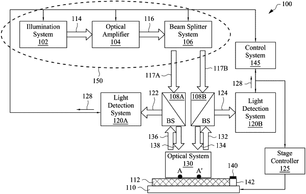
1. A method of manufacturing a semiconductor device, comprising:
transmitting two or more incident beams of light onto a first set of two or more first locations on top of a semiconductor substrate, respectively;
in response to the two or more incident beams of light, receiving two or more reflected beams of light from the first set of two or more first locations;
detecting, by two or more illumination detectors, the two or more reflected beams of light to generate two or more detected signals;
analyzing the two or more detected signals; and
determining, based on the analysis, whether a defect exists at the first set of the two or more first locations,
wherein the semiconductor substrate and a reference chip are mounted on a stage, wherein the two or more incident beams of light are focused on the reference chip, and wherein two or more second reflected beams of light are received from the reference chip respectively by the two or more illumination detectors for calibration thereof.
|