US 12,119,243 B2
Plasma etching chemistries of high aspect ratio features in dielectrics
Keren J. Kanarik, Los Altos, CA (US); Samantha Siamhwa Tan, Newark, CA (US); Yang Pan, Los Altos, CA (US); and Jeffrey Marks, Saratoga, CA (US)
Assigned to Lam Research Corporation, Fremont, CA (US)
Filed by Lam Research Corporation, Fremont, CA (US)
Filed on Feb. 2, 2023, as Appl. No. 18/163,522.
Application 18/163,522 is a continuation of application No. 16/979,372, granted, now 11,594,429, previously published as PCT/US2019/021761, filed on Mar. 12, 2019.
Claims priority of provisional application 62/644,095, filed on Mar. 16, 2018.
Prior Publication US 2023/0187234 A1, Jun. 15, 2023
Int. Cl. H01L 21/67 (2006.01); H01L 21/683 (2006.01)
CPC H01L 21/67069 (2013.01) [H01L 21/67109 (2013.01); H01L 21/6833 (2013.01)] 5 Claims
OG exemplary drawing
 
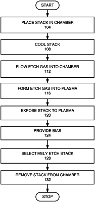
1. A method for etching a stack, comprising:
a) cooling the stack to a temperature below −20° C.;
b) flowing an etch gas into the etch chamber, wherein the etch gas comprises at least one of SiF4, TaF5, BrF5, AsF5, NF5, PF5, NbF5, BiF5, UF5, SiCl2, CrO2Cl2, TaCl4, HfCl4, TiCl3(1), CoCl2(1), TiCl3, CCl4, CBr2F2, C2F5Br, H2O, H2O2, BCl3, NH3, SiF4, CrO2Cl2, SiCl4, TiCl2, TiCl3, CoCl2, and TiCl2;
c) generating a plasma from the etch gas; and
d) selectively etching features in the stack with respect to a patterned mask, wherein the stack is comprised of alternating layers of silicon oxide and polysilicon.