| CPC H01L 21/4857 (2013.01) [G03F 7/70 (2013.01); H01L 21/481 (2013.01); H01L 23/49822 (2013.01); H01L 23/49838 (2013.01); H01L 23/49894 (2013.01); H01L 24/24 (2013.01); H01L 24/25 (2013.01); H01L 27/14634 (2013.01); H01L 2224/24147 (2013.01); H01L 2224/24227 (2013.01); H01L 2224/25171 (2013.01); H01L 2224/2518 (2013.01); H01L 2924/14335 (2013.01); H01L 2924/1461 (2013.01)] | 20 Claims |

|
1. A method of manufacturing a semiconductor device, the method comprising:
forming a redistribution layer over a substrate;
applying a first dielectric material to the redistribution layer and the substrate, wherein the first dielectric material has a transmittance to a first energy of greater than 0.5%, the first dielectric material comprising:
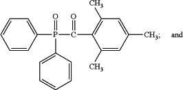
a first photoactive compound (PAC) with the following structure:
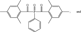
 a second PAC with at least two rings, the second PAC having the following structure:
 imaging the first dielectric material with the first energy.
|