| CPC H01L 21/304 (2013.01) [H01L 23/147 (2013.01); H01L 23/15 (2013.01); H01L 23/3121 (2013.01); H01L 23/3157 (2013.01); H01L 23/3185 (2013.01); H01L 23/3192 (2013.01); H01L 24/19 (2013.01); H01L 24/20 (2013.01); H01L 25/0655 (2013.01); H01L 25/072 (2013.01); H01L 21/561 (2013.01); H01L 2224/04105 (2013.01); H01L 2224/11 (2013.01); H01L 2224/12105 (2013.01); H01L 2224/16227 (2013.01); H01L 2224/32225 (2013.01); H01L 2224/73267 (2013.01); H01L 2224/92244 (2013.01)] | 20 Claims |

|
1. A method of manufacturing a semiconductor structure, comprising:
receiving a die comprising a top surface and a sacrificial layer covering the top surface;
disposing the die on a substrate;
disposing a molding surrounding the die;
removing a portion of the molding to expose a sidewall of the sacrificial laver;
removing the sacrificial layer from the die; and
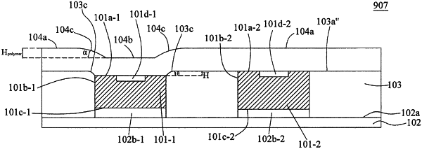
disposing a polymer over the die and the molding, wherein the polymer has a first bottom surface contacting the die and a second bottom surface contacting the molding, and the first bottom surface is at a level substantially same as the second bottom surface.
|