| CPC H01L 21/02603 (2013.01) [H01L 21/02636 (2013.01); H01L 21/265 (2013.01); H01L 29/0669 (2013.01)] | 7 Claims |

|
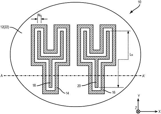
1. A method for manufacturing a nanowire structure comprising:
providing a substrate body, which is formed of a conducting material;
providing an implantation mask with an implantation opening over the substrate body, wherein a processing surface portion of a top surface of the substrate body is exposed through the implantation opening of the implantation mask;
applying ion implantation to the substrate body through the implantation opening, such that a portion of the substrate body, which extends from the exposed processing surface portion into the substrate body, is converted to an ion implantation region, wherein the ion implantation region is electrically insulating;
removing the implantation mask;
providing a patterned mask with a nanowire opening over the substrate body and the ion implantation region, wherein:
the patterned mask fully covers the ion implantation region; and
a nanowire surface portion of the top surface of the substrate body is exposed through the nanowire opening of the patterned mask; and
forming a nanowire over the exposed nanowire surface portion of the substrate body through the nanowire opening of the patterned mask, wherein:
the nanowire is not in contact with the ion implantation region; and
the nanowire is confined within the ion implantation region, such that the ion implantation region is configured to provide a conductivity barrier of the nanowire in the substrate.
|