| CPC H01J 37/3244 (2013.01) [H01J 37/32697 (2013.01); H01J 37/32715 (2013.01); H01J 37/32733 (2013.01); H01J 2237/3323 (2013.01); H01J 2237/334 (2013.01)] | 20 Claims |

|
1. A method of semiconductor processing comprising:
delivering a deposition precursor into a processing region of a semiconductor processing chamber;
depositing a layer of material on a substrate housed in the processing region of the semiconductor processing chamber, wherein the processing region is maintained at a first pressure during the depositing;
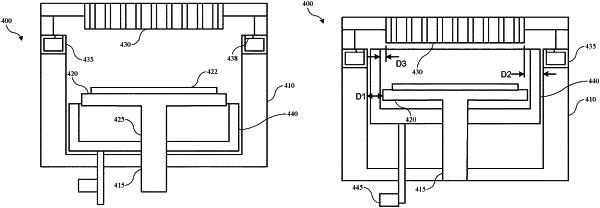
extending a baffle within the processing region, wherein the baffle modifies a flow path within the processing region;
forming a plasma of a treatment precursor within the processing region of the semiconductor processing chamber, wherein the processing region is maintained at a second pressure during the forming; and
treating the layer of material deposited on the substrate with plasma effluents of the treatment precursor.
|