| CPC G11C 16/102 (2013.01) [G11C 16/08 (2013.01); G11C 16/12 (2013.01)] | 20 Claims |

|
1. A flash memory device comprising:
a first memory cell;
a second memory cell on the first memory cell; and
a third memory cell between the first memory cell and the second memory cell,
wherein the first memory cell, the second memory cell and the third memory cell share a channel,
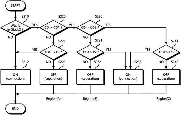
wherein the third memory cell is configured to block channel sharing between the first memory cell and the second memory cell based on a channel separation voltage provided in first to k-th program loops, and
wherein the third memory cell is configured to connect the channel sharing between the first memory cell and the second memory cell based on a channel connection voltage provided to the third memory cell in a (k+1)-th program loop.
|