| CPC G11C 16/08 (2013.01) | 20 Claims |

|
1. A memory device comprising;
a memory block connected with a plurality of wordlines;
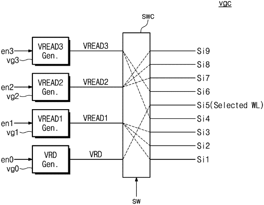
a voltage generating circuit configured to output a first non-selection voltage through a plurality of driving lines; and
an address decoding circuit configured to connect the plurality of driving lines with unselected wordlines of the plurality of wordlines,
wherein, during a wordline setup period for the plurality of wordlines,
the plurality of driving lines include first driving lines corresponding to first unselected wordlines among the unselected wordlines and second driving lines corresponding to second unselected wordlines among the unselected wordlines,
the voltage generating circuit is further configured to float the first driving lines when the first unselected wordlines reach a first target level,
the voltage generating circuit is further configured to float the second driving lines when the second unselected wordlines reach a second target level, and
the second target level is different from the first target level.
|