| CPC G11C 11/4096 (2013.01) [G11C 11/4076 (2013.01); G06F 13/1689 (2013.01); G11C 7/1066 (2013.01); G11C 7/1084 (2013.01); G11C 7/1093 (2013.01); G11C 7/14 (2013.01); G11C 11/4093 (2013.01)] | 20 Claims |

|
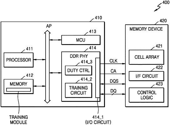
1. A system-on-chip comprising:
a memory device unit configured to operate in synchronization with an clock signal; and
a memory control unit configured to control an operation of the memory device unit,
wherein the memory control unit comprises:
a first receiver configured to compare a read reference voltage with a piece of data received through a first data line and configured to output a first piece of data;
a first duty adjuster connected to an output of the first receiver and configured to adjust a duty of the first piece of data;
a second receiver configured to compare the read reference voltage with a piece of data received through a second data line and configured to output a second piece of data;
a second duty adjuster connected to an output of the second receiver and configured to adjust a duty of the second piece of data; and
a training circuit configured to perform a training operation on pieces of data received through a plurality of data lines, to obtain a target read reference voltage for each of the pieces of data and correct a duty of each of the pieces of data based on a level of the target read reference voltage for each of the pieces of data,
wherein based on a result of the training operation, the duty of the first piece of data and the duty of the second piece of data are differently adjusted based on a level of a first target read reference voltage obtained for the first piece of data being different from a level of a second target read reference voltage obtained for the second piece of data.
|