| CPC G11C 11/4093 (2013.01) [G11C 11/4082 (2013.01); G11C 11/4076 (2013.01); G11C 11/408 (2013.01); G11C 11/4096 (2013.01)] | 20 Claims |

|
1. A semiconductor memory device comprising:
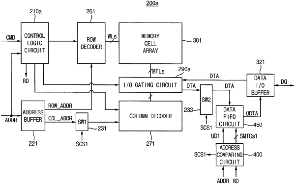
a memory cell array including a plurality of volatile memory cells coupled to a plurality of word-lines and a plurality of bit-lines;
a data input/output (I/O) buffer configured to provide the memory cell array with write data received in each of a plurality of write operations;
a data first-in/first-out (FIFO) circuit including a plurality of data FIFO buffers configured to store read data that is read from the memory cell array in each of a plurality of read operations, the data FIFO circuit configured to output data stored in one of the plurality of data FIFO buffers based on a plurality of sub matching signals;
an address comparing circuit configured to sequentially store a plurality of previous addresses that accompany first commands that designate a plurality of previous read operations, and configured to generate the plurality of sub matching signals based on a comparison of the previous addresses with a present address that accompanies a second command designating a present read operation; and
a control logic circuit configured to receive the first commands and the second command and configured to provide a read signal to the address comparing circuit in response to the first commands and the second command designating the plurality of previous read operations and the present read operation.
|