| CPC G09G 5/10 (2013.01) [G06F 1/3265 (2013.01); G09G 3/2007 (2013.01); G09G 3/3208 (2013.01); G09G 3/3275 (2013.01); G09G 3/3696 (2013.01); G09G 2310/0267 (2013.01); G09G 2310/027 (2013.01); G09G 2310/0291 (2013.01); G09G 2310/061 (2013.01); G09G 2310/08 (2013.01); G09G 2320/0276 (2013.01); G09G 2320/0673 (2013.01); G09G 2330/021 (2013.01); G09G 2330/022 (2013.01); G09G 2330/028 (2013.01); G09G 2340/0435 (2013.01)] | 20 Claims |

|
1. A display device comprising:
a display panel including a scan line, a data line, and a pixel connected to the scan line and the data line;
a gate driver configured to supply a scan signal to the scan line; and
a source driver configured to supply a data voltage to the data line,
wherein the source driver includes:
a gamma voltage generator configured to generate gamma voltages having voltage levels different from each other in response to a gamma enable signal;
a digital-to-analog converter configured to generate the data voltage corresponding to a gray scale value using the gamma voltages; and
a source buffer configured to output the data voltage to the data line, wherein the gamma voltage generator includes:
a first resistor string configured to set a voltage range of the gamma voltages;
a second resistor string configured to set tab gamma voltages corresponding to some of the gamma voltages within the voltage range;
gamma buffers configured to output the tab gamma voltages; and
a third resistor string including tabs respectively connected to output terminals of the gamma buffers, the third resistor string being configured to divide a voltage between the tabs to generate the gamma voltages,
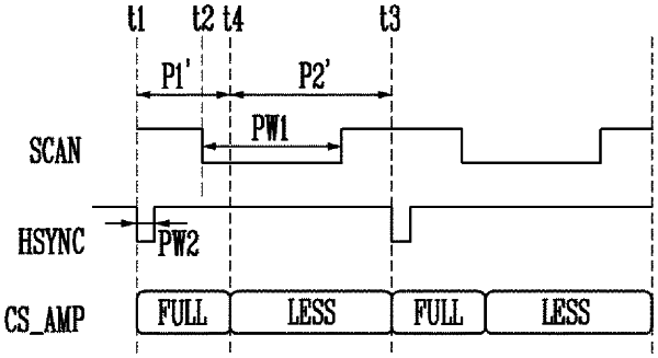
wherein the gamma voltage generator, in response to the gamma enable signal, outputs the tab gamma voltages during a part of a horizontal time and stops outputting some of the tab gamma voltages during a rest of the horizontal time, and
wherein the scan signal has a turn-off voltage level in the part of the horizontal time.
|