| CPC G09G 3/3233 (2013.01) [G09G 3/2007 (2013.01); G09G 3/2096 (2013.01); G09G 2300/0465 (2013.01); G09G 2300/0819 (2013.01); G09G 2300/0852 (2013.01); G09G 2300/0861 (2013.01); G09G 2310/0202 (2013.01); G09G 2310/08 (2013.01); G09G 2330/028 (2013.01)] | 20 Claims |

|
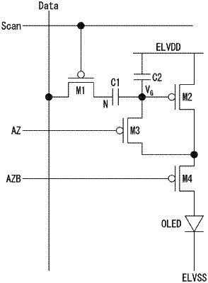
1. A pixel circuit configured to supply a current to a light emitting device so that the light emitting device emits light of a desired grayscale, the pixel circuit comprising:
a first transistor having a first terminal connected to a data line and to which a data signal is applied and a gate terminal connected to a scan line and to which a scan signal is applied;
a third transistor having a gate terminal connected to a second terminal of the first transistor and a second terminal connected to the light emitting device;
a capacitor having a second terminal commonly connected to the second terminal of the first transistor and the gate terminal of the third transistor; and
a second transistor having a second terminal commonly connected to a first terminal of the capacitor and a first terminal of the third transistor, a first terminal connected to a first power supply voltage, and a gate terminal connected to an emission line to which an emission signal is applied,
wherein, in a pre-charge period of a single operation cycle period, a gate voltage node of the third transistor is charged with an initial voltage, and a source voltage node of the third transistor is charged with the first power supply voltage, and
wherein, in a data input period following a threshold voltage sampling period of the single operation cycle period, the first transistor maintains a turned-on state by the scan signal, the second transistor maintains a turned-off state by the emission signal, the data signal is applied to the gate terminal of the third transistor through the first transistor and the third transistor maintains a turned-off state and coupling occurs by parasitic capacitors seen at the gate voltage node and the source voltage node.
|