| CPC G09G 3/32 (2013.01) [G09G 3/3233 (2013.01); G09G 3/20 (2013.01); G09G 2300/0408 (2013.01); G09G 2300/0426 (2013.01); G09G 2300/0439 (2013.01); G09G 2310/0278 (2013.01); G09G 2310/0286 (2013.01); G09G 2330/04 (2013.01)] | 18 Claims |
|
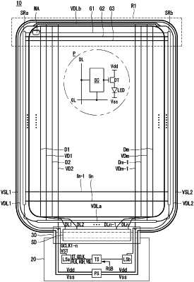
1. A display panel comprising:
an active area including at least one module area; and
a bezel area positioned outside the active area,
wherein the active area comprises a pixel array,
wherein each pixel in the pixel array includes a light emitting diode, a thin film transistor, and a connection electrode connecting the light emitting diode to the thin film transistor,
wherein the at least one module area is configured to have a light-transmissive area including at least one insulation layer between adjacent pixels of the pixel array,
wherein the at least one insulation layer comprises a first planarizing film disposed between the thin film transistor and the connection electrode,
wherein the first planarizing film is disposed in the light-transmissive area and the adjacent pixels of the pixel array,
wherein the bezel area comprises shift registers of a gate driver, the shift registers of the gate driver positioned on both sides of the active area to generate a gate signal to be supplied to the pixel array.
|