| CPC G09G 3/32 (2013.01) [G09G 3/2007 (2013.01); G09G 2300/0809 (2013.01); G09G 2310/061 (2013.01); G09G 2310/067 (2013.01); G09G 2320/0233 (2013.01)] | 10 Claims |

|
1. A display device, comprising:
a plurality of light emitting elements; and
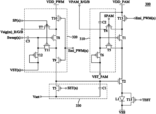
a plurality of driving circuits, each of the driving circuits is configured to generate a driving current to drive one of the light emitting elements to emit light, wherein each of the driving circuits comprises:
a first transistor, wherein the first transistor is a P type-transistor;
a second transistor, wherein the second transistor is an N-type transistor, wherein the second transistor is configured to control timing of a rising edge of the driving current in an emission period, wherein the second transistor is directly connected to the one of the light emitting elements, and wherein the driving current flows from a first system high voltage terminal sequentially through the first transistor, the second transistor and the one of the light emitting elements to a system low voltage terminal;
a reset circuit, configured to reset a voltage level of a gate terminal of the second transistor;
a first control circuit, configured to control the first transistor to adjust pulse amplitude of the driving current; and
a second control circuit, configured to control the second transistor to adjust a pulse width of the driving current, and configured to control the second transistor, according to a corresponding one of a plurality of sweep signals, to adjust a phase of the driving current,
wherein each of the driving circuits provides the driving current at different time points according to the sweep signals.
|