| CPC G09G 3/32 (2013.01) [G09G 3/3233 (2013.01); G09G 2310/0278 (2013.01); G09G 2330/028 (2013.01)] | 20 Claims |

|
1. A display device comprising:
a first pixel connected to a data line, a first power source, and a second power source;
a second pixel connected to the data line, the first power source, and the second power source;
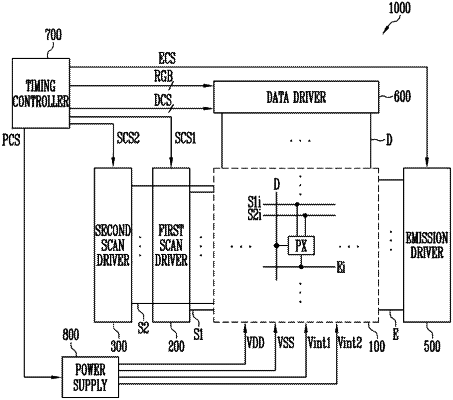
a first scan driver to supply a first scan signal to the first and second pixels;
a second scan driver to supply a second scan signal to the first and second pixels;
a first initialization power line to supply a first initialization voltage; and
a second initialization power line to supply a second initialization voltage,
wherein the first pixel comprises:
a first transistor connected between a first node and a second node and having a gate electrode connected to a third node;
a second transistor to be turned on in response to the first scan signal, the second transistor being connected between the data line and the first node;
a third transistor to be turned on in response to the second scan signal, the third transistor being connected between the second node and the third node;
a first light emitting element having an anode electrode and a cathode electrode, the anode electrode of the first light emitting element connected to the second node;
a fourth transistor connected between the third node and the first initialization power line to transfer the first initialization voltage of the first initialization power line to the third node; and
a fifth transistor connected between the anode electrode and the second initialization power line to transfer the second initialization voltage of the second initialization power line to the anode electrode, and
wherein the second scan signal has a signal characteristic different from that of the first scan signal.
|