| CPC G06F 7/60 (2013.01) [G06F 7/57 (2013.01); G06N 3/08 (2013.01); H01L 27/1207 (2013.01); H01L 27/1225 (2013.01); H01L 27/124 (2013.01); H01L 27/1255 (2013.01); H01L 29/78648 (2013.01); H01L 29/7869 (2013.01); H10B 12/00 (2023.02)] | 20 Claims |

|
1. A semiconductor device comprising:
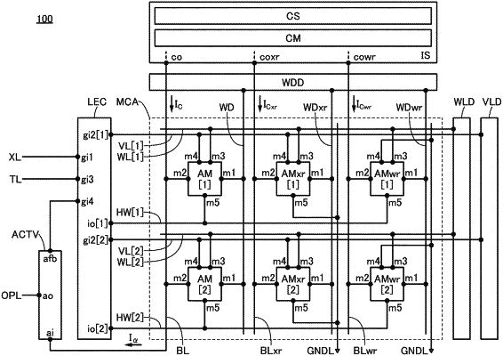
a first circuit configured to perform first arithmetic operation using a first data and a second data according to a predetermined formula, in order to output a first result;
a second circuit configured to output a first potential using a first current corresponding to the first result;
a third circuit configured to perform second arithmetic operation using the first result, the second data, and teacher data, and to output a second potential corresponding to a second result of the second arithmetic operation; and
a first memory cell electrically connected to the third circuit, the first memory cell storing a third potential,
a second memory cell electrically connected to the first circuit, the second memory cell configured to store a fourth potential corresponding to the first data,
a third memory cell electrically connected to the first circuit and the third circuit, the third memory cell configured to store a fifth potential corresponding to the second data,
wherein the teacher data is data input from outside to the third circuit,
wherein the first circuit is configured to output the first current into the second circuit,
wherein the third circuit is configured to receive the first potential output from the second circuit,
wherein the first result is a result of the first arithmetic operation using the first data and the second data, and
wherein the second result is configured to be input to the third memory cell to update the second data.
|