| CPC G06F 7/5443 (2013.01) [G06F 17/16 (2013.01); H03K 19/20 (2013.01); H03M 1/38 (2013.01)] | 21 Claims |

|
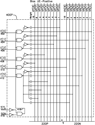
1. A Bias Unit Element (UE) receiving an E digital input with an enable bit and generating charge coupled to a charge transfer bus comprising charge transfer lines, each charge transfer line having an associated weight, the Bias UE comprising:
a plurality of logic gates, each logic gate having an input coupled to an E digital input bit and the enable bit and generating a positive output and a negative output;
the positive output coupled through a first charge transfer capacitor to a positive charge transfer line, the negative output coupled through a second charge transfer capacitor to a negative charge transfer line;
each charge transfer line having an associated binary weight, the binary weight for each charge transfer line including at least weights 1, 2, 4, 8, and 16.
|