US 12,118,241 B2
Memory controller, memory system, and operating method thereof
Do Hun Kim, Icheon (KR)
Assigned to SK hynix Inc., Icheon (KR)
Filed by SK hynix Inc., Icheon (KR)
Filed on Apr. 16, 2021, as Appl. No. 17/233,210.
Application 17/233,210 is a continuation in part of application No. 16/871,775, filed on May 11, 2020, granted, now 11,194,520.
Application 17/233,210 is a continuation in part of application No. 16/781,309, filed on Feb. 4, 2020, granted, now 11,366,763.
Application 17/233,210 is a continuation in part of application No. 16/111,044, filed on Aug. 23, 2018, granted, now 11,068,408.
Application 16/871,775 is a continuation of application No. 15/976,651, filed on May 10, 2018, granted, now 10,684,796, issued on Jun. 16, 2020.
Claims priority of application No. 10-2017-0141380 (KR), filed on Oct. 27, 2017; application No. 10-2018-0000363 (KR), filed on Jan. 2, 2018; and application No. 10-2019-0023135 (KR), filed on Feb. 27, 2019.
Prior Publication US 2021/0232343 A1, Jul. 29, 2021
Int. Cl. G06F 3/06 (2006.01); G06F 11/10 (2006.01); G06F 12/10 (2016.01); G11C 29/04 (2006.01); G11C 29/52 (2006.01)
CPC G06F 3/0659 (2013.01) [G06F 3/0604 (2013.01); G06F 3/068 (2013.01); G06F 11/1048 (2013.01); G06F 11/1068 (2013.01); G06F 12/10 (2013.01); G06F 2212/1008 (2013.01); G06F 2212/608 (2013.01); G06F 2212/657 (2013.01); G11C 2029/0411 (2013.01); G11C 29/52 (2013.01)] 16 Claims
OG exemplary drawing
 
1. A memory controller, comprising:
a cache memory;
a buffer memory device storing logical-physical address mapping information loaded from a nonvolatile memory device;
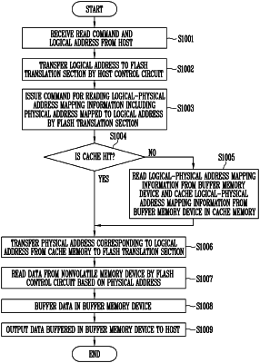
a host control circuit configured to receive a read command and a logical address from a host, issue a first command, in response to the read command, to read out mapping information corresponding to the logical address, from the buffer memory device when the mapping information corresponding to the logical address is cache-missed in the cache memory, and cache the mapping information from the buffer memory device in the cache memory; and
a flash translation layer configured to receive the logical address from the host control circuit, and issue a second command to read a physical address corresponding to the logical address from the mapping information cached in the cache memory.