| CPC G06F 3/0446 (2019.05) [G06F 3/0412 (2013.01); H10K 50/865 (2023.02); H10K 59/40 (2023.02); H10K 59/50 (2023.02); G06F 2203/04112 (2013.01)] | 5 Claims |

|
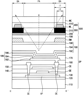
1. A display device comprising:
a light emitting diode disposed in a light emitting area;
an encapsulation layer disposed on the light emitting diode;
an electrode layer disposed on the encapsulation layer;
a black matrix disposed on the encapsulation layer, wherein the black matrix is between the electrode layer and the encapsulation layer;
a viewing angle adjusting layer directly disposed on the electrode layer; and
a window cover disposed on the viewing angle adjusting layer,
wherein the viewing angle adjusting layer includes a material which absorbs a portion of light generated from the light emitting diode,
wherein a light absorption rate of the material is independent of a voltage applied to the viewing angle adjusting layer, and
wherein at least some of the material is included in a portion of the viewing angle adjusting layer which is spaced apart from the light emitting diode in a plan view.
|