| CPC G06F 1/1609 (2013.01) [H10K 50/841 (2023.02); H10K 50/8426 (2023.02); G06F 1/1637 (2013.01); H10K 71/00 (2023.02)] | 20 Claims |

|
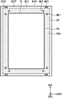
1. A display device defining a longitudinal direction, a width direction perpendicular to the longitudinal direction, and a thickness direction perpendicular to the longitudinal and width directions, and comprising:
a display panel, including:
a display region including a plurality of pixels;
a non-display region around the display region; and
a first indicia and a second indicia disposed in the non-display region, the first indicia and the second indicia separated and spaced apart from each other when viewed in a plan view; and
a window disposed on the display panel and, including:
a transmission region overlapping the display region;
a light blocking region overlapping the non-display region; and
a third indicia disposed in the light blocking region;
wherein when viewed in a plan view, the third indicia disposed in the light blocking region does not overlap with the first indicia and the second indicia separated from each other in the non-display region, and
wherein the third indicia does not overlap the display panel in the thickness direction.
|