| CPC G02F 1/1368 (2013.01) [H10K 59/1201 (2023.02); H10K 59/1213 (2023.02)] | 4 Claims |

|
1. A display device comprising:
a display region including a thin-film transistor;
a frame region surrounding the display region;
a terminal section provided in the frame region;
a resin layer provided above a base;
an inorganic insulating layer provided on the resin layer and including openings;
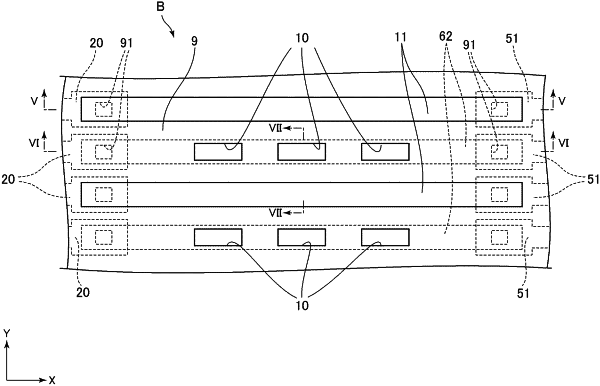
conductive patterns provided on the inorganic insulating layer in locations except for locations over the openings; and
a bending portion provided between the display region and the terminal section and provided with the resin layer, the inorganic insulating layer, and a plurality of the conductive patterns,
wherein the conductive patterns electrically connect the terminal section and the thin-film transistor together; and
a plurality of the openings is provided at intervals between the plurality of the conductive patterns along an extending direction of the conductive patterns.
|