| CPC G02B 27/0172 (2013.01) [H10K 50/11 (2023.02); H10K 50/844 (2023.02); H10K 50/85 (2023.02); H10K 77/10 (2023.02); G02F 2201/121 (2013.01); G02F 2201/123 (2013.01)] | 20 Claims |

|
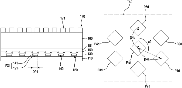
1. A display device comprising:
a substrate;
a pixel electrode on the substrate;
a display element emitting a light and disposed on the pixel electrode;
a common electrode on the display element;
an encapsulation layer on the common electrode;
an air between the display element and the encapsulation layer; and
a plurality of diffraction patterns on the encapsulation layer,
wherein:
the plurality of diffraction patterns includes a first diffraction pattern and a second diffraction pattern arranged along a first direction with a first period,
a width of a cross section of each of the first diffraction pattern and the second diffraction pattern is defined as a first length,
the first length and the first period satisfy Inequality (1):
0.4≤d1/DP1≤1, (1)
where DP1 is the first period, and d1 is the first length.
|