| CPC C25D 21/12 (2013.01) [C25D 7/123 (2013.01); C25D 17/001 (2013.01); G05B 13/027 (2013.01)] | 17 Claims |

|
1. A system comprising:
a first semiconductor processing station configured to deposit a material on a first semiconductor wafer;
a second semiconductor processing station configured to perform measurements indicative of a thickness of the material after the material has been deposited on the first semiconductor wafer; and
a controller configured to perform operations comprising:
receiving the measurements from the second semiconductor processing station;
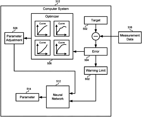
generating an error calculation using the measurements and a target value for the first semiconductor wafer;
providing the error calculation to an optimizer that is configured to use one or more sensitivity curves that relate the error calculation to a change in an operating parameter of the first semiconductor processing station;
providing the change in the operating parameter to a trained model, wherein the trained model is configured to generate an output that adjusts the operating parameter of the first semiconductor processing station such that the thickness of the material is closer to a target thickness of the material; and
causing the first semiconductor processing station to deposit the material on a second semiconductor wafer using the operating parameter as adjusted by the output.
|