| CPC C23C 16/45527 (2013.01) [C23C 16/4408 (2013.01); H01L 21/02126 (2013.01); H01L 21/31116 (2013.01)] | 18 Claims |

|
1. An area-selective deposition method comprising:
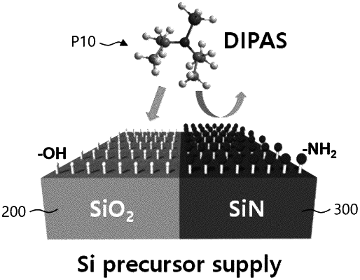
providing a substrate structure comprising a silicon oxide area having a surface with a first functional group and a silicon nitride area having a surface with a second functional group; and
performing an atomic layer deposition (ALD) process on the substrate structure in a chamber to selectively form a silicon oxide layer on the silicon oxide area among the silicon nitride area and the silicon oxide area, the ALD process comprising:
a first supply step of supplying an aminosilane-based silicon precursor into the chamber;
a first purge step of purging the chamber with a first purge gas;
a second supply step of supplying an oxygen-containing source into the chamber; and
a second purge step of purging the chamber with a second purge gas,
wherein the ALD process further comprises introducing a reaction inhibitor selectively on the silicon nitride area among the silicon oxide area and the silicon nitride area, and
wherein an inhibitor precursor material for the reaction inhibitor forms Si(CH3)3 on the silicon nitride area.
|