| CPC B32B 17/10036 (2013.01) [B32B 17/10504 (2013.01); B32B 17/10761 (2013.01); G02F 1/1334 (2013.01); B32B 2305/55 (2013.01); B32B 2605/006 (2013.01); H05B 3/84 (2013.01)] | 18 Claims |

|
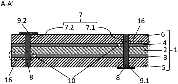
1. A multilayer film with electrically switchable optical properties, at least comprising, arranged areally in the following order:
a first carrier film,
a first electrically conductive layer,
an active layer,
a second electrically conductive layer, and
a second carrier film,
wherein
the multilayer film has within its area at least one first cutout and the at least one first cutout protrudes in the form of a through-hole through all layers of the multilayer film such that the at least one first cutout penetrates into the active layer,
the first cutout is filled with an electrically conductive filler compound, which electrically conductingly contacts the first electrically conductive layer within the first cutout, and
a first busbar electrically conductingly contacts the electrically conducting filler compound,
wherein the multilayer film has within its area at least one second cutout in the form of a through-hole through all layers of the multilayer film, the second cutout is filled with an electrically conductive filler compound, which electrically conductingly contacts the second electrically conductive layer within the second cutout, and a second busbar electrically conductingly contacts the electrically conducting filler compound, and
wherein
the first and second cutouts protrude through all layers of the multilayer film, at least one first layer-free separating line is arranged in the first electrically conductive layer, wherein said at least one first layer-free separating line separates a first electrically insulated edge region comprising the at least one first cutout or the at least one second cutout from a primary surface of the first electrically conductive layer, and
at least one second layer-free separating line is arranged in the second electrically conductive layer, wherein said at least one second layer-free separating line separates a second electrically insulated edge region from a primary surface of the second electrically conductive layer, wherein the second electrically insulated edge region of the second electrically conductive layer includes those of the first and second cutouts that do not extend within the first electrically insulated edge region of the first electrically conductive layer.
|