| CPC H03F 3/245 (2013.01) [H03F 1/56 (2013.01); H03F 3/193 (2013.01); H03F 2200/18 (2013.01); H03F 2200/451 (2013.01)] | 9 Claims |
|
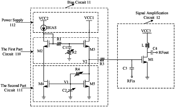
1. A bias circuit of a power amplifier, comprising a first part circuit, a second part circuit, and a power supply, wherein
the power supply is connected with a power supply end of the first part circuit and configured to supply power to the first part circuit;
two ends of the first part circuit are connected in parallel with two ends of the second part circuit, one end of the parallel connection is connected with a gate of a first transistor of the power amplifier in a signal amplification circuit, the first part circuit is configured to provide a first bias voltage to the gate of the first transistor, the second part circuit is configured to provide a second bias voltage to the gate of the first transistor, and the first bias voltage and the second bias voltage are superimposed to provide a stable bias voltage to the gate of the first transistor; and
an impedance of the bias circuit is in a preset impedance range;
wherein
the first part circuit comprises a second transistor, a third transistor, a first resistor, a second resistor, and a first capacitor
a drain of the second transistor is connected with the power supply, and the drain and a gate of the second transistor are connected to each other; a source of the second transistor is connected with one end of the second part circuit; the gate of the second transistor is connected to a gate of the third transistor through the first resistor, and is also connected to a ground terminal through the first capacitor;
a drain of the third transistor is connected with the power supply, and a source of the third transistor is connected with another end of the second part circuit and also connected with the gate of the first transistor;
the second resistor is a variable resistor; and
the first capacitor is connected with the ground terminal through the second resistor.
|