| CPC H02J 50/80 (2016.02) [H02J 50/12 (2016.02)] | 21 Claims |
|
1. A power receiver comprising:
an input circuit comprising a receiver coil, wherein the receiver coil is arranged to extract power from a power transfer signal;
a transmitter circuit,
wherein the transmitter circuit is arranged to transmit a first plurality of data symbols to a power transmitter by load modulating the power transfer signal,
wherein the transmitter circuit is arranged to transmit data symbols to the power transmitter during a power transfer phase using a selected communication mode;
a detector circuit, wherein the detector circuit is arranged to monitor the power transfer signal so as to detect the first variation of the power transfer signal; and
a selector circuit,
wherein the selector circuit is arranged to select a first communication mode as the selected communication mode if the first variation of the power transfer signal is detected,
wherein the selector circuit is arranged to select a second communication mode as the selected communication mode if the first variation of the power transfer signal is not detected,
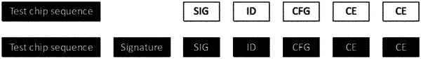
wherein the first communication mode comprises modulating each data symbol of the first plurality of data symbols by a sequence of modulation load values,
wherein the sequence of modulation load values corresponds to at least one chip sequence of the first plurality of chip sequences,
wherein the plurality of data symbols comprises a request for the first variation of the power transfer signal,
wherein the second communication mode does not modulate any data symbol by a sequence of modulation load values corresponding to any chip sequence of the first plurality of chip sequences.
|