| CPC G11C 16/16 (2013.01) [G11C 16/0483 (2013.01); G11C 16/08 (2013.01); G11C 16/107 (2013.01); G11C 16/24 (2013.01)] | 29 Claims |
|
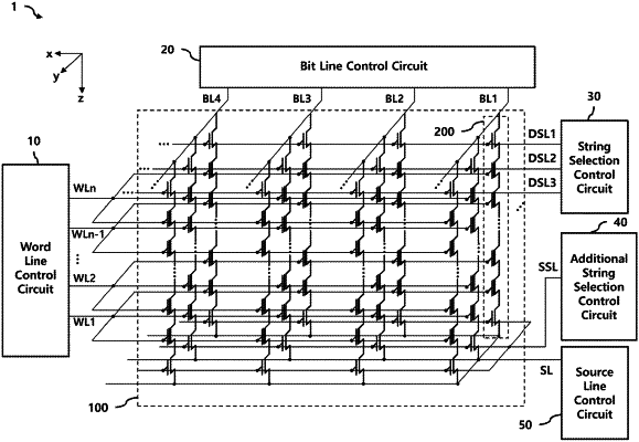
1. A flash memory device comprising:
a cell array including a first NAND string having a plurality of first flash memory cells having control gates connected to a plurality of word lines, respectively, and a first bit line selection switch connecting the plurality of first flash memory cells to a first bit line according to a control of a first string selection line; and
a control circuit configured to control a first erase operation for erasing a selected flash memory cell among the plurality of first memory cells,
wherein the control circuit controls a voltage difference between the first bit line and the first string selection line to have a first value for generating gate induced drain leakage (GIDL) at the first bit line selection switch, and controls a voltage of a control gate of the selected flash memory cell and a voltage of a control gate of an unselected flash memory cell among the plurality of first flash memory cells to be different from each other,
wherein the cell array further comprises a second NAND string having a plurality of second flash memory cells having control gates connected to the plurality of word lines, respectively, and a second bit line selection switch connecting the plurality of second flash memory cells to the first bit line according to a control of a second string selection line, and
wherein the control circuit controls a voltage difference between the first bit line and the second string selection line to have a second value that is smaller than the first value during the first erase operation.
|