| CPC G11C 16/0483 (2013.01) [G11C 7/1006 (2013.01)] | 12 Claims |
|
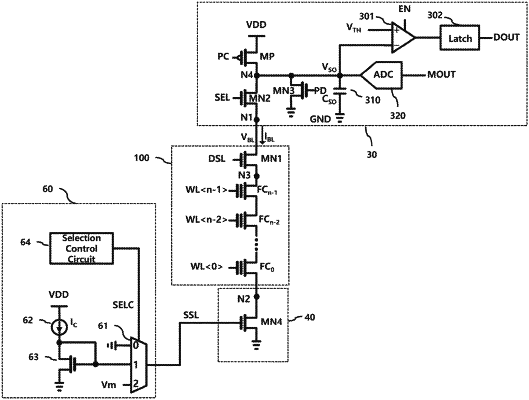
1. A semiconductor memory device comprising:
a cell array including a plurality of memory cells connected between a first bit line and a source line, the plurality of memory cells being connected to a plurality of word lines, respectively;
a computation control circuit configured to control a first bit line current between the first bit line and the source line to have a constant value during a computation operation; and
an output circuit including a first computation capacitor whose charge amount is changed according to the first bit line current during the computation operation,
wherein an amount of charge that flows between the first bit line and the source line during the computation operation depends on both data stored in a memory cell among the plurality of memory cells according to a first data and a voltage of a word line connected to the memory cell provided according to a second data,
wherein the computation operation includes a multiplication and accumulation (MAC) operation having a result corresponding to a sum of respective products of elements of the first data and elements of the second data,
wherein the MAC operation is performed by reading each of the plurality of memory cells storing a value corresponding to an element of the first data by providing a word line voltage determined according to a corresponding element of the second data and a read voltage which is selected from one or more threshold voltages used to determine values stored in corresponding memory cells, and
wherein a voltage of the first computation capacitor corresponds to a result of a MAC operation of the first data and the second data after the computation operation.
|