| CPC G09G 3/3266 (2013.01) [H10K 59/1213 (2023.02); G09G 2300/0426 (2013.01); G09G 2300/0439 (2013.01); H10K 50/18 (2023.02)] | 20 Claims |
|
1. A display device comprising:
a substrate having a display area and a non-display area;
a pixel disposed in the display area of the substrate; and
a gate driving circuit disposed in the non-display area of the substrate and connected to a transistor of the pixel,
wherein the gate driving circuit comprises a plurality of stages,
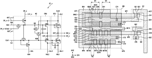
wherein each of the plurality of stages in the gate driving circuit includes:
a node control unit;
a carry output unit connected to the node control unit and outputting a carry signal applied to at least one of a previous stage or a subsequent stage;
a pull-up transistor connected to a set node of the node control unit through a first gate electrode; and
a pull-down transistor connected to a reset node of the node control unit through a second gate electrode,
wherein a width of a first channel region of the pull-up transistor is greater than a width of a second channel region of the pull-down transistor,
wherein the carry output unit includes a first transistor connected to the set node through a gate electrode and a second transistor connected to the reset node through a gate electrode, and
wherein the pull-up transistor further includes a first counter gate electrode connected to the first gate electrode, and the pull-down transistor further includes a second counter gate electrode connected to a different node than the second gate electrode.
|