| CPC G06F 3/0412 (2013.01) [G06F 3/04164 (2019.05); G06F 3/0445 (2019.05); G06F 3/0446 (2019.05)] | 6 Claims |
|
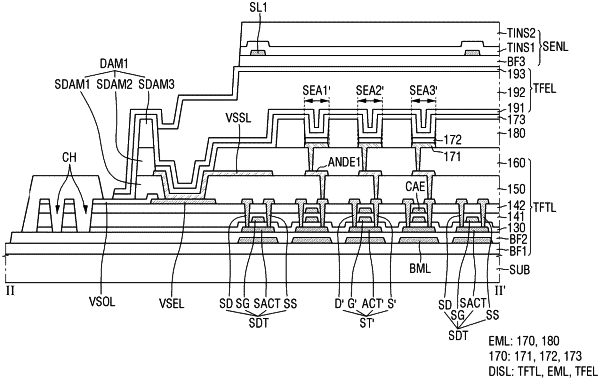
1. A display device, comprising:
a display panel including a front portion, a first side portion which extends from a first side of the front portion, a second side portion which extends from a second side of the front portion, and a corner portion disposed between the first side portion and the second side portion, and
wherein the display panel further includes:
a first display area disposed in the front portion and including a plurality of first light-emitting elements; and
a second display area disposed in the corner portion, and
wherein the second display area includes:
a plurality of second light-emitting elements;
a plurality of thin film transistors, each of the plurality of thin film transistors is connected to corresponding one of the plurality of second light-emitting elements; and
a plurality of scan driving transistors of a scan driving circuit for outputting scan signals, and
wherein at least one thin film transistor among the plurality of thin film transistors is disposed between adjacent scan driving transistors among the plurality of scan driving transistors in one direction,
wherein the second display area further includes a first power supply line to which a first power supply voltage is applied, and
wherein the first power supply line overlaps at least one scan driving transistor of the plurality of scan driving transistors.
|