| CPC G02B 6/0031 (2013.01) [G02B 6/0068 (2013.01); G02B 6/0083 (2013.01)] | 18 Claims |
|
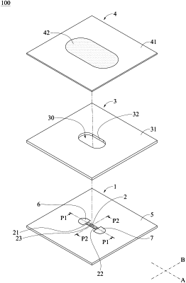
1. A light guide module, comprising:
a circuit board;
a light emitting unit, comprising a first light emitting unit and a second light emitting unit, wherein the first light emitting unit and the second light emitting unit are arranged on the circuit board along a first axis, the light emitting unit has a second axis, and the second axis is substantially perpendicular to the first axis;
a light guide plate, having a through hole and a light conducting area, wherein the through hole is surrounded by a hole wall, the light guide plate is located on the circuit board and the light emitting unit is located in the through hole, there is a first gap between the first light emitting unit and the adjacent hole wall along the first axis, there is a second gap between the first light emitting unit and the adjacent hole wall along the second axis, and the first gap is larger than the second gap, there is a fourth gap between the second light emitting unit and the adjacent hole wall along the second axis, wherein on the second axis, the light conducting area around the through hole comprises a second sub-light conducting area and a fourth sub-light conducting area;
a film, having a light transmitting area and a light adjusting portion, wherein the light adjusting portion is located in the light transmitting area, the light conducting area corresponds to the light transmitting area, and the through hole corresponds to the light adjusting portion;
a lower adhesion member, arranged under the light guide plate and arranged around the light emitting unit; and
a microstructure area, arranged on the second sub-light conducting area adjacent to the second gap and the fourth sub-light conducting area adjacent to the fourth gap, wherein the microstructure area is arranged above the lower adhesion member.
|