| CPC G01S 7/4861 (2013.01) [G01S 7/4865 (2013.01); G01S 17/89 (2013.01); H04N 23/682 (2023.01)] | 54 Claims |
|
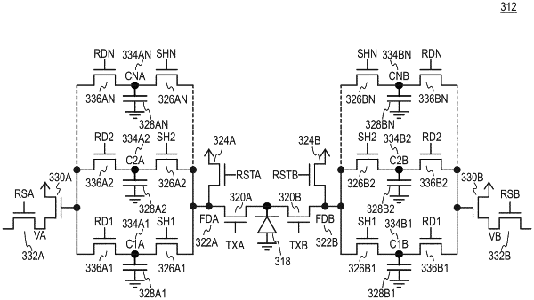
1. A time-of-flight pixel circuit, comprising:
a photodiode configured to generate charge in response to modulated light emitted from a light source and reflected from an object to the photodiode;
a first transfer transistor coupled to the photodiode;
a second transfer transistor coupled to the photodiode, wherein the first transfer transistor is configured to transfer a first portion of charge from the photodiode in response to a first modulation signal, wherein the second transfer transistor is configured to transfer a second portion of charge from the photodiode in response to a second modulation signal, wherein the second modulation signal is an inverted first modulation signal;
a first floating diffusion coupled to the first transfer transistor to receive the first portion of charge in response to the first modulation signal;
a first plurality of memory nodes;
a first plurality of sample and hold transistors, wherein each one of the first plurality of sample and hold transistors is coupled between a respective one of the first plurality of memory nodes and the first transfer transistor;
a first output source follower transistor;
a first plurality of readout transistors, wherein each one of the first plurality of readout transistors is coupled between the respective one of the first plurality of memory nodes and a gate of the first output source follower transistor; and
a first row select transistor coupled to the first output source follower transistor,
wherein:
a first one of the first plurality of memory nodes is coupled to the first floating diffusion through a first one of the first plurality of sample and hold transistors during a first subframe,
a second one of the first plurality of memory nodes is coupled to the first floating diffusion through a second one of the first plurality of sample and hold transistors during a second subframe, and
the first one of the first plurality of memory nodes is coupled to the gate of the first output source follower transistor through a first one of the first plurality of readout transistors during the second subframe.
|