| CPC B81B 7/02 (2013.01) [B81C 1/00158 (2013.01); B81B 2201/0264 (2013.01); B81B 2203/0127 (2013.01); B81B 2203/0315 (2013.01); B81B 2203/0346 (2013.01); B81B 2203/04 (2013.01); B81B 2203/051 (2013.01); B81B 2207/012 (2013.01); B81B 2207/115 (2013.01); B81C 2201/013 (2013.01); B81C 2203/0109 (2013.01); B81C 2203/032 (2013.01)] | 16 Claims |
|
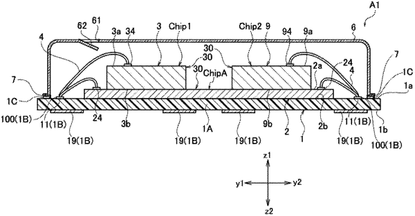
1. A MEMS module comprising:
a first MEMS element and a second MEMS element each including a movable portion which is a portion of a substrate including a hollow portion formed therein, the movable portion configured to warp in shape according to an air pressure difference between an internal air pressure inside the hollow portion and external air pressure outside the hollow portion; and
an electronic component configured to calculate a change in external air pressure outside the substrate by using an amount of warpage of the movable portion of at least one of the first MEMS element and the second MEMS element,
wherein the amount of warpage of the movable portion according to the external air pressure differs between the first MEMS element and the second MEMS element, and
wherein a film thickness of the movable portion adjoining the hollow portion of the second MEMS element is larger than a film thickness of the movable portion adjoining the hollow portion of the first MEMS element.
|