US 12,114,567 B2
Photoelectric devices having charge transport layer including first charge transport material and second charge transport material and sensors and electronic devices
Seok-Hwan Hong, Seoul (KR); Sung Jun Park, Yongin-si (KR); Kyung Bae Park, Hwaseong-si (KR); Sung Young Yun, Suwon-si (KR); and Chul Joon Heo, Busan (KR)
Assigned to Samsung Electronics Co., Ltd., Gyeonggi-Do (KR)
Filed by Samsung Electronics Co., Ltd., Suwon-si (KR)
Filed on Jan. 6, 2023, as Appl. No. 18/150,888.
Application 18/150,888 is a continuation of application No. 16/887,405, filed on May 29, 2020, granted, now 11,563,186, issued on Jan. 24, 2023.
Claims priority of application No. 10-2019-0138740 (KR), filed on Nov. 1, 2019; and application No. 10-2020-0045432 (KR), filed on Apr. 14, 2020.
Prior Publication US 2023/0157167 A1, May 18, 2023
Int. Cl. H01L 29/08 (2006.01); H10K 85/40 (2023.01); H10K 85/60 (2023.01); H10K 30/30 (2023.01); H10K 39/32 (2023.01)
CPC H10K 85/6572 (2023.02) [H10K 85/40 (2023.02); H10K 85/615 (2023.02); H10K 85/626 (2023.02); H10K 85/654 (2023.02); H10K 85/6574 (2023.02); H10K 30/30 (2023.02); H10K 39/32 (2023.02)] 20 Claims
OG exemplary drawing
 
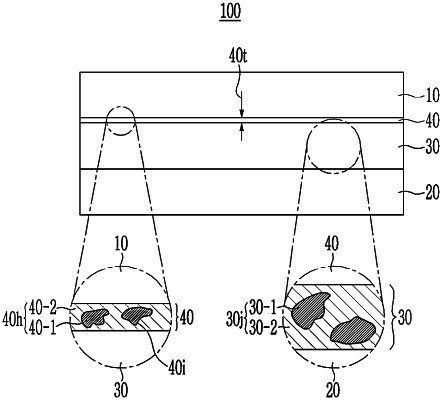
1. A thin film for a photoelectric device, the thin film comprising:
a first charge transport material and a second charge transport material that collectively define a heterojunction,
wherein the thin film is configured to facilitate transfer of charge carriers that are separated in a photoelectric conversion layer of the photoelectric device to reduce a quantity of remaining charge carriers in the photoelectric conversion layer, and
wherein the first charge transport material and the second charge transport material are mixed, and
wherein the first charge transport material and the second charge transport material have a same nitrogen-containing ring.