| CPC H10K 59/1315 (2023.02) [G09G 3/3233 (2013.01); G09G 3/3266 (2013.01); H01L 27/0296 (2013.01); H10K 50/8426 (2023.02); H10K 59/1213 (2023.02); H10K 59/122 (2023.02); H10K 59/124 (2023.02); H10K 59/40 (2023.02)] | 20 Claims |
|
1. An organic light emitting display apparatus comprising:
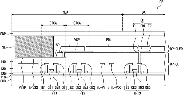
a base layer comprising a display area and a non-display area adjacent to the display area;
a circuit element layer comprising a first transistor in the display area including a first semiconductor pattern, a first transistor electrode electrically connected to the first semiconductor pattern, and a second transistor electrode electrically connected to the first semiconductor pattern, a first control electrode overlapping the first semiconductor pattern, a lower insulating layer covering the first control electrode, an upper insulating layer disposed on the lower insulating layer, a power supply line to receive a common voltage, an auxiliary power supply pattern electrically connected to the power supply line, a voltage line to receive a source voltage greater than the common voltage and electrically connected to the first transistor electrode, and an auxiliary voltage pattern electrically connected to the voltage line; and
a display element layer comprising a first electrode on the circuit element layer and electrically connected to the second transistor electrode, a light emitting layer on the first electrode, and a second electrode on the light emitting layer and electrically connected to the power supply line;
wherein the power supply line and the voltage line are located between the lower insulating layer and the upper insulating layer,
wherein the auxiliary power supply pattern and the auxiliary voltage pattern are disposed on the upper insulating layer and are in contact with the upper insulating layer.
|