| CPC H10K 59/131 (2023.02) [H10K 50/844 (2023.02); H10K 50/8445 (2023.02); H10K 71/70 (2023.02); H10K 59/40 (2023.02); H10K 2102/311 (2023.02)] | 12 Claims |
|
1. A display device comprising:
a substrate;
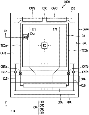
a display area including a plurality of pixels on the substrate;
a first area disposed adjacent to the display area on the substrate;
an encapsulation layer disposed on the first area and the display area;
a buffer layer disposed on the encapsulation layer;
a plurality of touch conductors disposed on the buffer layer and in the display area;
a crack detection line disposed on the buffer layer and in the first area, wherein
the crack detection line comprises a same material as at least one of the plurality of touch conductors, and
the crack detection line comprises a first curved portion and a second curved portion where an extension direction of the crack detection line is reversed, and
the first curved portion and the second curved portion area spaced apart from each other and face each other.
|