| CPC H10K 59/131 (2023.02) [H10K 59/122 (2023.02); H10K 59/80517 (2023.02); H10K 2102/102 (2023.02); H10K 2102/103 (2023.02); H10K 2102/351 (2023.02)] | 19 Claims |
|
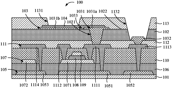
1. An array substrate, comprising:
a substrate;
a planarization layer disposed on a side of the substrate and provided with a first via hole;
a connection layer comprising a connecting portion, wherein the connecting portion is disposed in the first via hole and extends to a surface of the planarization layer; and
an anode layer disposed on a surface of the connecting portion away from the planarization layer,
wherein the connecting portion comprises:
a first sub-connecting portion covering the first via hole; and
a second sub-connecting portion disposed on the surface of the planarization layer, wherein there is a gap between the first sub-connecting portion and the second sub-connecting portion, the anode layer covers the first sub-connecting portion, the second sub-connecting portion, and a part of the planarization layer located at the gap, and the first sub-connecting portion and the second sub-connecting portion are connected by the anode layer.
|