| CPC H10K 59/124 (2023.02) [H01L 29/66742 (2013.01); H01L 29/7869 (2013.01); H10K 59/131 (2023.02); H10K 59/1201 (2023.02)] | 3 Claims |

|
1. A display device comprising:
a substrate;
a first transistor formed on the substrate; and
a second transistor formed on the substrate,
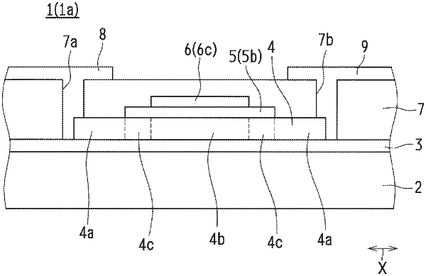
the first transistor including:
a first oxide semiconductor layer formed on the substrate;
a first gate insulating layer formed on the first oxide semiconductor layer; and
a first gate electrode formed on the first gate insulating layer,
the first oxide semiconductor layer including:
a first conductive region provided with conductivity;
a first central resistance region positioned below the first gate electrode; and
a first lateral resistance region provided between the first conductive region and the first central resistance region, and positioned outside the first gate electrode, and
the first central resistance region being larger in resistance than the first lateral resistance region, and the first gate insulating layer of the first transistor covering only the first central resistance region and the first lateral resistance region of the first oxide semiconductor layer, wherein
the second transistor includes:
a second oxide semiconductor layer formed on the substrate;
a second gate insulating layer formed on the second oxide semiconductor layer; and
a second gate electrode formed on the second gate insulating layer,
the second oxide semiconductor layer includes:
a second conductive region provided with conductivity; and
a second central resistance region positioned below the second gate electrode,
the second gate insulating layer matches the second central resistance region and the second gate electrode in shape, and
the second central resistance region is provided in contact with the second conductive region.
|