| CPC H10K 59/122 (2023.02) [H10K 50/822 (2023.02); H10K 50/865 (2023.02); H10K 50/828 (2023.02); H10K 59/1201 (2023.02); H10K 59/131 (2023.02); H10K 71/00 (2023.02); H10K 2102/3026 (2023.02)] | 21 Claims |

|
1. A display element comprising:
a thin film transistor (TFT) layer;
a plurality of lower reflective electrodes;
a plurality of banks each having a linear shape;
a plurality of active layers each having a linear shape and formed between adjacent banks of the plurality of banks; and
an upper transparent electrode formed on each of the plurality of active layers,
wherein the plurality of lower reflective electrodes, the plurality of banks, the plurality of active layers, and the upper transparent electrode are on an upper side of the TFT layer,
each of the plurality of active layers is provided in common to the plurality of lower reflective electrodes and forms a plurality of same color pixels,
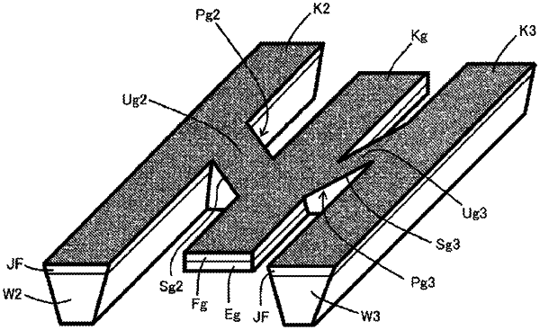
each of the plurality of banks is inversely tapered toward a TFT layer side,
a height of each of the plurality of banks with reference to the TFT layer is greater than a height of the upper transparent electrode with reference to the TFT layer,
one or more cut lines having a locally reduced height with reference to the TFT layer are formed in a bank of the plurality of banks positioned between adjacent active layers of the plurality of active layers,
the upper transparent electrode formed on one of the adjacent active layers and the upper transparent electrode formed on the other one of the adjacent active layers are electrically connected via a conductive electrode formed in the one or more cut lines,
the one or more cut lines and the conductive electrode are formed in each of the plurality of banks, and
a first cut line and a second cut line of the adjacent banks with one active layer of the plurality of active layers interposed therebetween are offset with respect to an extending direction of the plurality of banks in a plan view.
|