| CPC H10K 59/1216 (2023.02) [H10K 59/1213 (2023.02); H10K 59/126 (2023.02); H10K 59/131 (2023.02); H01L 27/1225 (2013.01); H01L 27/124 (2013.01); H01L 27/1255 (2013.01); H01L 27/1259 (2013.01); H01L 29/78633 (2013.01); H01L 29/7869 (2013.01); H10K 59/1201 (2023.02)] | 10 Claims |
|
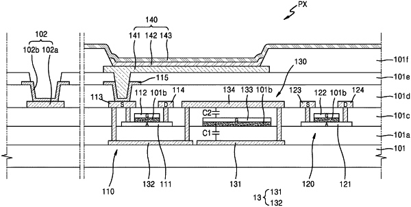
1. An organic light-emitting display apparatus comprising:
a display unit comprising an organic light-emitting element, a driving transistor electrically connected to the organic light-emitting element, and a capacitor electrically connected to the driving transistor, the capacitor comprising:
a first conductive layer disposed on a substrate;
a second conductive layer having a first portion and a second portion spaced apart from the first portion, the first portion interposed between the first conductive layer and the substrate facing a first surface of the first conductive layer; and
a third conductive layer disposed to face a second surface of the first conductive layer opposing the first surface of the first conductive layer, wherein
a portion of the third conductive layer is in direct contact with an upper surface of the first portion of the second conductive layer through a first contact hole that passes through a first insulating layer between the first portion of the second conductive layer and the first conductive layer such that the third conductive layer is electrically connected to the first portion of the second conductive layer, and
the first portion of the second conductive layer overlaps the organic light-emitting element.
|