| CPC H10K 59/1213 (2023.02) [H10K 59/1216 (2023.02); H10K 59/131 (2023.02); G09G 2300/0819 (2013.01); G09G 2300/0823 (2013.01)] | 20 Claims |

|
1. A display substrate, comprising a base substrate and a plurality of pixel units arranged in an array on the base substrate, with the array having a first side and a second side, which are opposite to each other, wherein
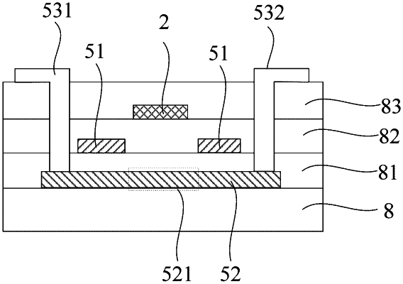
each pixel unit comprises at least one constant voltage terminal and at least one dual-gate transistor, each dual-gate transistor comprises two gates which are spaced apart, and a part of an active region of the dual-gate transistor, which is located between the two gates, is an intermediate part;
except the pixel units closest to the first side, each pixel unit further comprises a compensation structure, the compensation structure is connected to one constant voltage terminal of the pixel unit where the compensation structure is located, and compensates for the at least one dual-gate transistor of a pixel unit adjacent to the pixel unit where the compensation structure is located in a direction toward the first side;
the compensation structure overlaps and is insulated from the intermediate part of the dual-gate transistor for which the compensation structure compensates, and the compensation structure and the two gates of the dual-gate transistor for which the compensation structure compensates are located on a same side of the active region of the dual-gate transistor with respect to the base substrate; and
the pixel units closest to the second side are redundant pixel units which are not used for display.
|